Using the Vishay IL300, a stable, linear optocoupler

Among optocouplers, those providing the greatest thermal and time stability are those with two matched photodetectors in the package with the photoemitter. This configuration lets the deveice be used in a servo circuit.  The current from one of the photodetectors (P1) is used to estimate the photocurrent that is delivered to the other photodetector (P2). The circuit placed around this device provides a drive current to the photoemitter which is servoed to be that which produces the desired current in P1, thus producing this same desired current in P2, to the matching accuracy of P1 and P2.

The Vishay IL300 analog optocoupler is a good example of such an optocoupler. Its data sheet www.vishay.com/poptocouplers/list/product-83622/ shows a servo circuit.

The linearity of this example circuit is given as only 0.01 percent, when the bias current to the photoemitter is 10 mA and the modulation on top of this is +-4 mA.

The drift with temperature of this example circuit is only +-0.005% per degree C typically, +-0.05% per degree C maximum.     The data sheet shows the frequency response of the IL300 from photoemitter current to photodetector current is DC to 200 KHz (at 3 db rolloff, -45 degree phase delay).

The photodetector current / photoemitter current is typically 0.007 Using this ratio, the external circuit (op amp output to negative input) voltage gain is about (30,000 / 100) * 0.007 = about 2.

The example circuit (Fig. 13) uses a LM201 op amp with external compensation of 100 pf (between pins 1 and 8).  This gives the op amp an open loop gain of 0.5 at about 300 KHz The total circuit’s open loop gain will trherefore be about 1 at 300 KHz.

The added phase lag from the photoemitter to photodetector response is 45 degrees at 200 KHz.  So it will be somewhat more than this at 300 KHz., maybe 60 degrees.

The op amp’s open-loop phase lag at 300 MHz is about 90 degrees, so very roughly the total unity gain phase lag might be about 150 degrees.  this is less than 180 degrees so the circuit should be stable but it should have quite a bit of square wave overshoot.   My main point is one must design the servo circuit carefully.  One must avoid instability due to phase lag in the photoemitter to photodetector path.  Vishay has an app note 55:  http://www.vishay.com/docs/83711/appn55.pdf  showing in Fig. 6 that you can use a capacitor from the op amp out[put to the feedback input (the negative input) to achieve stability, by providing a non-phase-lagged feedback path for the higher frequencies.

When the right component values are used, keeping the feedback loop phase shift under about 120 degrees at the unity open-loop-gain frequency, the op amp in this case can be a unity-gain-stable op amp.  Interestingly, however, in Fig. 6, the uncompensated OP-07 is used.  I an skeptical of this curcuit as shown, because it does not have a dominant pole.  I suspect that they just omitted an external compensating capacitor in the schematic.

As always, one should SPICE model the circuit.  in particular, one can learn a lot from the servo’s open loop Bode plot.  I like Liner Technology’s LTSpice for this purpose.

Your thoughts?

Larry Miller


High bandwidth high voltage bipolar driver

High voltage power supplies normally use a switched waveform (usually square wave) generator with transformer, inductor or sometimes even a capacitor-diode multiplying ladder.  The output voltage is divided down to a reasonable voltage and compared with a reference voltage using a error amplifier (analog amplifier such as an op amp).  The error is filtered and applied to control the output amplitude of the switched waveform generator.  This is the control loop; it the filter is chosen to provide responsiveness and stability.

This type of supply can be made to follow varying command voltage just as it can be proportional to a reference voltage.  However, for stability, the bandwidth of the control loop must be well under the switching frequency, usually no more than one tenth of the switching frequency.  Most switchers switch at under one MHz., thus limiting the output frequency that can be produced to less than 100 KHz.

If it is desired to produce a high-voltage waveform, for example -1200 volts to +1200 volts, that has for example a passband of DC to 1 MHz., then the following approach can be used.

Start with DC supplies of -1250 volts and +1250 volts.  Use a main tote-pole current output structure consisting of two current-drive circuits in series:  one current drive circuit sources current from the positive supply and the other sinks output current to the negative supply.

Choose an output drive transistor with the required voltage rating of 2400 volts and sufficient bandwidth, to be the main element of the current-drive circuit.  I choose the IXYS IXTV02N250S N-Channel MOSFET.

There are no P-channel MOSFET’s available commercially with this voltage capability, so I use the same circuit and transistor for both current drive circuits.

Now, the main problem is to provide the gate drive to the two MOSFET’s.  The output of this drive circuit must float at up to 1250 volts either side of ground.

The Avago HCNW4562 analog optocoupler is well suited for this purpose.  It can couple an analog signal across a voltage difference of up to +-1414 volts on a continuous basis.  And it has a bandwidth of 13 MHz.

The gate of each of the MOSFET’s can be driven by a totem pole consisting of the output transistors of two HCNW4562’s.  The lower HCNW4562 transistor sinks to the source supply voltage of the MOSFET, and the upperHCNW4562  transistor sources to a voltage say 15 volts above this source supply voltage.  This totem pole provides bipolar current drive to the MOSFET gate.  The gate has a capacitance to source of typically 116 pf, and to the drain of 3 pf.  A 1 MHz. sine wave on he output, that causes MOSFET gate voltage variation of +-2 volts, and output voltage variation of +-500 volts will thus cause a current draw at the gate of +-11 milliamps.  This is within the output drive capability of the optocouplers.

As usual, an error amplifier produces the difference between the divided output waveform and the command waveform.  This is filtered and used to drive one or the other circuit of the main totem pole.

The key enabling technologies for this topology are the high bandwidth analog optocouplers, and the high voltage high bandwidth MOSFET’s.

Implementing this topology requires a complex design, and there are many remaining issues: to name a few, power dissipation, how to supply power to the upper optocoupler output transistor, ensuring loop stability given the phase delays of the optocouplers and the MOSFET’s, how to add current limiting, and more.

Starting with a topology concept such as this, one should flesh out the details and subject the design to a critical review.  Then model the circuit.  When satisfied with the model results, build it and test it.  And iterate as needed.

Larry Miller


.


Low voltage noise JFET input synthesized op amp

Many of my preamplifiers have been driven by high-impedance (i.e. over 1 kilohm) sources, such as broadband stub antennas, capacitive proximity sensors, Faraday cups, photodiodes, and APD’s (avalanche photodiodes).  For this type of source, I have always wished for an FET-input op amp that had low equivalent input voltage noise like the best bipolar-input op amps.

A bipolar-input op amp could load down the source, reducing the voltage it presents to the op amp input, and also would inject too much noise current (typically on the order of a picoamp per root Hz) back to the source, producing an added equivalent noise voltage, which would be proportional to the source impedance.  FET op amps have a very high input resistance, which avoids loading the source, and also they only inject femtoamps of noise current per root Hz back into the source.

An FET-input op amp is the best choice for high-impedance sources.  However the commercially available ones have equivalent input noise voltages of about 5 nanovolts per root Hz.

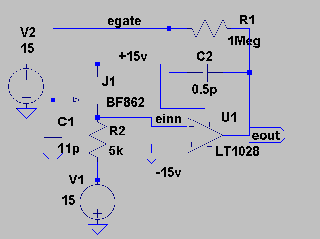
Now, in http://www.linear.com/product/LT1028, Linear Technology shows us how create an effective FET-input op amp from a discrete junction FET and a bipolar op amp.

The circuit is

Synthetic FET input op amp

The data sheet for the discrete N-channel junction FET BF862  is  http://www.nxp.com/documents/data_sheet/BF862.pdf

C1 represents the source impedance.  the circuit will work if the source impedance is partially (a resistor and capacitor in series or parallel) or totally resistive, also.

The JFET is used as a source follower to lower the effective source resistance seen by the bipolar op amp LT1028.  The total equivalent input noise voltage for this synthesized FET-input op amp is the quadrature sum of the two noise voltage sources, the JFET and the op amp:  sqrt (0.8e-9^2 + 0.85e-9^2) = 1.17 nanovolt/root Hz.

The discrete FET does add phase lag to the forward transfer function of the synthesized amplifier.  However, the FET has a transition frequency of 715 MHz., so phase lag at 50 MHz. will probably be under 0.1 radians (6 degrees).  The gain-bandwidth product of the LT1028 op amp is 50 MHz., so the closed loop gain even in a unity gain configuration will be under one, for frequencies above 50 MHz., and thus excess phase lag above 50 Mhz will not cause instability.

The BF862 is a particularly good JFET for this purpose, having low voltage noise and high bandwidth.  Other op amps could be used instead of the LT1028, where needed, but if they have a gain-bandwidth product above 50 MHz the synthesized amplifier may not be stable.

As always, this amplifier should be modeled in Spice (I suggest using LTSpice  IV http://www.linear.com/designtools/software/#Amp), using worst-case parameters.

Larry MIller